Plated Through Holes PTH Processes in the PCB factory---Electroless Chemical Copper Plating
Almost all PCBs with double layers or multi-layers use plated through holes (PTH) to connect the conductors between inner layers or out layers, or to hold components lead wires. To achieve that, good connected paths are needed for current to flow through the holes. However, prior to plating process, through holes is non-conductive due to printed circuit boards are composed by non-conductive composite substrate material (epoxy-glass, phenolic-paper, polyester-glass, etc.). To produce conduciveness though the hole paths, about 25 microns (1 mil or 0.001 in.) of copper or more specified by circuit board designer is required to deposited electrolytically on the walls of the holes to create enough connection.
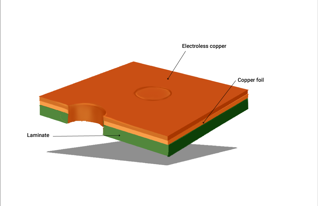
Before the electrolytical copper plating, the first step is the chemical copper plating, also called electroless copper deposition, to obtain initial conductive layer on the wall of the holes of printed wiring boards. An autocatalytic oxidation-reduction reaction happens on the surface of non-conducting substrate of through holes. Upon the wall a very thin coat of copper about 1-3 micrometer thickness is chemically deposited. Its purpose is to make the hole surface conductive enough to permit further build-up with copper deposited electrolytically to the thickness specified by the wiring board designer. Besides copper, we can use palladium, graphite, polymer, etc. as conductors. But copper is the best option for the electronic developer on the normal occasions.
As the IPC-2221A table 4.2 says that the minimum copper thickness being applied by electroless copper plating method on the walls of PTH for average copper deposition is 0.79 mil for class Ⅰ and Class Ⅱ and 0.98 mil for class Ⅲ.
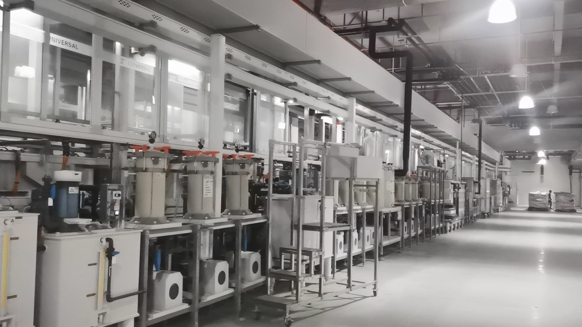
The chemical copper deposition line is fully computer controlled and the panels are carried through a series of chemical and rinsing baths by the overhead crane. At first, the pcb panels are pre-treated, removing all residue from drilling and providing excellent roughness and electro positiveness for the chemical deposition of copper. The vital step is the permanganate desmear process of the holes. During the treatment process, a thin layer of epoxy resin is etched away from the edge of the inner layer and the walls of the holes, to ensure adhesion. Then all hole walls are immersed in active bathes to get seeded with micro-particles of palladium in active baths. The bath is maintained under normal air agitation and the panels are constantly moving through the bath to remove potential air bubbles that may have formed inside the holes. A thin layer of the copper deposited onto the entire surface of the panel and drilled holes after the palladium bathing. Electroless plating with the use of palladium provides for the strongest adhesion of the copper coating to the fiberglass. At the end an inspection is carried out to check the porosity and the thickness the copper coat.
Each step is critical to the overall process. Any mishandling in the procedure can cause the entire batch of PCB boards to get wasted. And the final quality of pcb lies significantly in those steps mentioned here.
Now, with conductive holes, electrical connection between inner layers and out layers established for circuit boards. The next step is to grow the copper in those holes and top and bottom layers of the wiring boards to the specific thickness - copper electroplating.
Full automated chemical electroless copper plating lines in PCB ShinTech with Cutting edge PTH Technology.
Post time: Jul-18-2022