Posted: Feb 15, 2022
Categories: Blogs
Tags: pcb, pcbs, pcba, pcb assembly, smt, stencil
What is a PCB Stencil?
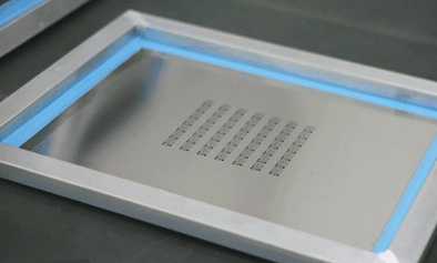
PCB Stencil, also known as Steel mesh, is a sheet of stai
nless steel with laser cut openings used to transfer an accurate amount of solder paste to an accurate designated position on a bare PCB for surface mount components placement. The stencil is composed of stencil frame, wire mesh and steel sheet. There are many holes in the stencil, and the positions of these holes correspond to the positions that need to be printed on the PCB. Main function of stencil is to accurately deposit the right amount of solder paste on pads so that the solder joint between the pad and the component is perfect in terms of the electrical connection and mechanical strength.
When in use, place the PCB under the stencil, Once the
stencil is properly aligned on top of the board, solder paste is applied over the openings.
Then the solder paste is leaked to the PCB surface through small holes at the fixed position on the stencil. When the steel foil is separated from the board, solder paste will remain on surface of the circuit board, ready for placement of surface mount devices (SMDs). The less solder paste is blocked on the stencil, the more it is deposited on the PCB. This process can be repeated accurately, so it makes the SMT process faster and more consistency and ensure the cost-effective of PCB Assembly.
What is a PCB Stencil made of?
A SMT stencil is mainly made of stencil frame, mesh and
stainless-steel sheet, and glue. Commonly applied stencil frame is the frame sticked to the wire mesh with glue, which is easy to obtain uniform steel sheet tension, which is generally 35 ~ 48N / cm2. Mesh is for fixing steel sheet and frame. There are two types of meshes, stainless steel wire mesh and polymer polyester mesh. The former can provide stable and sufficient tension but easy to deform and wear off. The later however can last long comparing to stainless steel wire mesh. Generally adopted stencil sheet is 301 or 304 stainless steel sheet that obviously improves the performance of the stencil through its excellent mechanical properties.
Manufacturing Method of Stencil
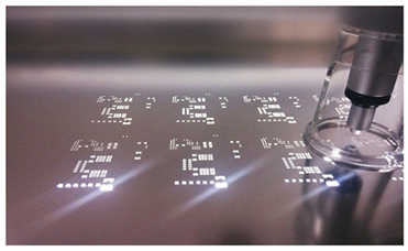
There are seven types of stencils and three methods for manufacturing stencils: chemical etching, laser cutting and electroforming. Generally used is laser steel stencil. Las
er stencil is the most commonly used in SMT industry, which is characterized is:
The data file is directly used to reduce the manufacturing error;
The opening position accuracy of SMT stencil is extremely high: the whole process error is ≤± 4 μ m;
The opening of SMT stencil has geometry, which is conduci
ve to the printing and molding of solder paste.
Laser cutting process flow: film making PCB, taking coordinates, data file, data processing, laser cutting, grinding. The process is with high data production accuracy and little influence of objective factors; Trapezoidal opening is conducive to demoulding, it can be used for precision cutting, price cheapness.
General requirements and principles of PCB Stencil
1. To get a perfect print of solder paste on the PCB pads, the specific position and specification shall ensure high opening accuracy, and the opening shall be in strict accordance with the specified opening method referred to fiducial marks.
2. To avoid solder defects like bridging and solder beads, the independent opening shall designed slightly smaller than the PCB pad size. the total width shall not exceed 2mm. The area of the PCB pad should always be greater than two-thirds of the area of the inside of the aperture wall of the stencil.
3. When stretching the mesh, strictly control it, and pa
y special attention to the opening range, which must be horizontal and centered.
4. With the printing surface as the top, the lower opening of the mesh shall be 0.01mm or 0.02mm wider than the upper opening, that is, the opening shall be inverted conical to facilitate the effective release of solder paste and reduce the cleaning times of the stencil.
5. The mesh wall must be smooth. Especially for QFP and CSP with spacing less than 0.5mm, the supplier is required to conduct electropolishing during the manufacturing process.
6. Generally, the stencil opening specification and shape of SMT components are consistent with the pad, and the opening ratio is 1:1.
7. Accurate thickness of the stencil sheet ensures the release
of the desired amount of solder paste through the opening. Extra solder deposition can cause solder bridging while less solder deposition will cause weak solder joints.
How to design a PCB Stencil?
1. 0805 package is recommended to cut the two pads of the opening by 1.0mm, and then make the concave circle B = 2 / 5Y; A = 0.25mm or a = 2 / 5 * l anti tin bead.
2. Chip 1206 and above: after the two pads are moved outward by 0.1mm respectively, make an inner concave circle B = 2 / 5Y; A = 2 / 5 * l anti tin bead treatment.
3. For PCB with BGA, the opening ratio of stencil with ball spacing of more than 1.0mm is 1:1, and the opening ratio of stencil with ball spacing of less than 0.5mm is 1:0.95.
4. For all QFP and SOP with 0.5mm pitch, the opening rati
o in the total width direction is 1:0.8.
5. The opening ratio in the length direction is 1:1.1, with 0.4mm pitch QFP, the opening in the total width direction is 1:0.8, the opening in the length direction is 1:1.1, and the outer rounding foot. Chamfer radius r = 0.12mm. The total opening width of SOP element with 0.65mm pitch is reduced by 10%.
6. When PLCC32 and PLCC44 of general products are perforated, the total width direction is 1:1 and the length direction is 1:1.1.
7. For general SOT packaged devices, the opening ratio
of large pad end is 1:1.1, the total width direction of small pad end is 1:1, and the length direction is 1:1.
How to Use a PCB Stencil?
1. Handle with care.
2. The stencil shall be cleaned before use.
3. Solder paste or red glue shall be applied evenly.
4. Adjust the printing pressure to the best.
5. To use pasteboard printing.
6. After the scraper stroke, it is best to stop for 2 ~ 3 seconds before demoulding, and set the demoulding speed not too fast.
7. Stencil shall be cleaned in time, stored well after usage.
Stencil Manufacture Service of PCB ShinTech
PCB ShinTech offers laser stainless steel stencils manufacture services. We make stencils with thicknesses of 100 μm, 120 μm, 130µm, 150 μm, 180 μm, 200 μm, 250 μm and 300 μm. The data file required to make the laser stencil must contain SMT solder paste layer, fiducial mark data, PCB outline layer and character layer, so we can check the front and back sides of the data, component category, etc.
If you require a quote please send your files and enquiry to sales@pcbshintech.com.
Post time: Jun-10-2022