PCB Fabrication & PCB Assembly Capabilities
PCB Manufacturing Capabilities
| Items | Standard PCB | Advanced PCB |
| Manufacturing Capacity | 40,000 m2 per month | 40,000 m2 per month |
| Layer | 1,2, 4, up to 10 layers | 1,2, 4, up to 50 layers |
| Material | FR-4, CEM-1, Aluminum, etc. | FR-4 (Normal to high Tg), High CTI FR-4, CEM-1, CEM-3, Polymide (PI), Rogers, Glass Epoxy, Aluminium Base, Rohs Compliant, RF, etc. |
| PCB type | Rigid | Rigid, Flexible, Rigid-Flexible |
| Min. Core Thickness | 4mil/0.1mm(2-12 layer), 2mil/0.05mm (≥13layer) | 4mil/0.1mm(2-12 layer), 2mil/0.06mm (≥13layer) |
| Prepreg Type | 1080, 2116, 765-8, 106, 3313, 2165, 1500 | 1080, 2116, 765-8, 106, 3313, 2165, 1500 |
| Max Board Size | 26''*20.8 '' /650mm*520mm | Customizable |
| Board Thickness | 0.4mm/16mil-2.4mm/96mil | 0.2mm/8mil-10.0mm/400mil |
| Thickness Tolerance | ±0.1mm (Board Thickness<1.0mm); ±10% (Board Thickness≥1.0mm) | ±0.1mm (Board Thickness<1.0mm); ±4% (Board Thickness≥1.0mm) |
| Dimensional deviation | ±0.13mm/5.2mil | ±0.10mm/4 mil |
| Warping Angle | 0.75% | 0.75% |
| Copper Thickness | 0.5-10 oz | 0.5-18 oz |
| Copper Thickness Tolerance | ±0.25 oz | ±0.25 oz |
| Min. Line Width/Space | 4mil/0.1mm | 2mil/0.05mm |
| Min. Drill Hole Diameter | 8mil/0.2mm (mechanical) | 4mil/0.1mm (laser), 6mil/0.15mm (mechanical) |
| PTH Wall Thickness | ≥18μm | ≥20μm |
| PTH Hole Tolerance | ±3mil/0.076mm | ±2mil/0.05mm |
| NPTH Hole Tolerance | ±2mil/0.05mm | ±1.5mil/0.04mm |
| Max. Aspect Ratio | 12:1 | 15:1 |
| Min. Blind/Buried Via | 4mil/0.1mm | 4mil/0.1mm |
| Surface Finish | HASL, OSP, Immersion Gold | HASL, OSP, Nickle, Immersion Gold, Imm Tin, Imm Silver, etc. |
| Solder Mask | Green, Red, White, Yellow, Blue, Black | Green, Red, White, Yellow, Blue, Black, Orange, Purple, etc. Customizable |
| Solder Mask offset | ±3mil/0.076mm | ±2mil/0.05mm |
| Silkscreen Color | Green, Red, White, Yellow, Blue, Black | Green, Blue, Black, White, Red, Purple, Transparent, Grey, Yellow, Orange, etc. Customizable |
| Silkscreen Min. Line Width | 0.006'' or 0.15mm | 0.006'' or 0.15mm |
| Impedance Control | ±10% | ±5% |
| Hole Location Tolerance | ±0.05mm, ±0.13mm (2nd drilled hole to 1st hole location) | ±0.05mm, ±0.13mm (2nd drilled hole to 1st hole location) |
| PCB Cutting | Shear, V-Score, Tab-routed | Shear, V-Score, Tab-routed |
| Tests and inspection | A.O.I., Fly Probe Testing, ET test, Microsection Inspection, Solderability Test, Impedance Test, etc. | A.O.I, Fly Probe Testing, ET test, Microsection Inspection, Solderability Test, Impedance Test, etc. |
| Quality Standard | IPC Class II | IPC Class II, IPC Class III |
| Certification | UL, ISO9001:2015, ISO14001:2015, TS16949:2009, RoHS etc. | UL, ISO9001:2008, ISO14001:2008, TS16949:2009, AS9100, RoHS, etc. |
PCB Assembly Capabilities
| Services | Turnkey-from bare boards manufacturing, Component sourcing, assembly, package, delivery; Kitted/partial turkey-partial processes of list above according to requires of customer. |
| Facilities | 15 in-house SMT lines, 3 in-house through-hole lines, 3 in-house final assembly lines |
| Types | SMT, Thru-hole, Mixed (SMT/Thru-hole), Single or double sided placement |
| Lead Time | Quickturn, Prototype or small amount: 3-7work days days (all parts are ready). Mass Order: 7-28 work days (all parts are ready); Scheduled delivery available |
| Testing on Products | X-ray Inspection, ICT (In-Circuit Testing), 100% BGA X-Ray Inspection, AOI Testing (Automated Optical Inspection), Testing Jig/Mold, Functional Test, Counterfeit Component Inspection (for kitted assembly type), etc. |
| PCB Specifications | Rigid, Metal Core, Flexible, Flex-Rigid |
| Quantity | MOQ: 1 pc. Prototype, small order, mass production |
| Parts Procurement | Turnkey, Kitted/ Partial Turnkey |
| Stencials | Laser cut stainless steel |
| Nano-coating available | |
| Soldering types | Leaded, Lead-free, RoHS Compliant, No-clean and Water Clean Fluxes |
| Files Needed | PCB: Gerber files (CAM, PCB, PCBDOC) |
| Components: Bill of Materials (BOM List) | |
| Assembly: Pick & Place file | |
| PCB Panel Size | Min. Size: 0.25*0.25 inch (6mm*6mm) |
| Max Size: 48*24 inch (1200mm*600mm) | |
| Components Details | Passive Down to 01005 size |
| BGA and Ultra-Fine (uBGA) | |
| Leadless Chip Carriers/CSP | |
| Quad Flat Package No-Lead (QFN) | |
| Quad Flat Package (QFP) | |
| Plastic Leaded Chip Carrier (PLCC) | |
| SOIC | |
| Package-On-Package (PoP) | |
| Small Chip Package (Fine Pitch to 0.02mm/0.8 mils) | |
| Double-sided SMT Assembly | |
| automatic placement of Ceramic BGA, Plastic BGA, MBGA | |
| Removing & Replacing BGA's & MBGA's, down to 0.35mm pitch, up to 45mm | |
| BGA Repair and Reball | |
| Part Removal and Replacement | |
| Cable and Wire | |
| Component package | Cut Tape, Tube, Reels, Partial Reel, Tray, Bulk, Loose Parts |
| Quality | IPC Class II / IPC Class III |
| Other Capabilities | DFM Analysis |
| Aqueous Cleaning | |
| Conformal coating | |
| PCB Testing Services |
Quality Management
Quality is our highest priority. PCB ShinTech has a targeted approach to make sure that your PCBs are produced and assembled with maximum quality and consistency. Nothing at PCB ShinTech is left to chance. We work hard at every functional level to make sure that every process is defined and work instruction is documented so that we can consistently provide the same top-notch products and services to our customers.
1. Understand customer expectations and needs.
2. Continuously create and deliver new values to customers.
3. Response to customers’ complain promptly. If we experience a problem, we treat every such event as an opportunity to learn what went wrong, and how to prevent a re-occurrence.
4. Establish well-functional quality management system and improve the effectiveness of the system continuously.
We back the quality of your PCBs and PCBA by preparing the right tooling, using the right equipment, buying in the right materials, implementing the right processing, and hiring and training the right operators. Each order goes through the same tightly controlled processes with an aim to not only increase efficiencies for the benefit of our customers but with the fundamental goal of consistently delivering quality product built to the customer’s expectations and board specifications.
In-house facilities and equipment
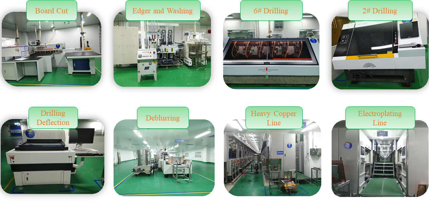
In-house facilities of PCB ShinTech are capable of 40,000 m2 per month of PCB fabrication. At the same time PCB ShinTech has 15 SMT lines and 3 through-hole lines in-house. Your PCBs are never produced by the lowest bidder out of a large pool of factories. To achieve exceptional quality performance from PCB assembly, we continuously invest in latest equipment that allows the exact precision necessary for the entire assembly process, including X Ray, solder paste, pick and place and more.
Staff training
Each of PCB ShinTech 's manufacturing and assembly facilities has fully trained inspectors, because our most important goal is delivering quality. Operator training is critical. It is the duty of every operator to check the boards as they go through their process, and we make sure that they have received fully training and gain the necessary expertise.
Inspection and test
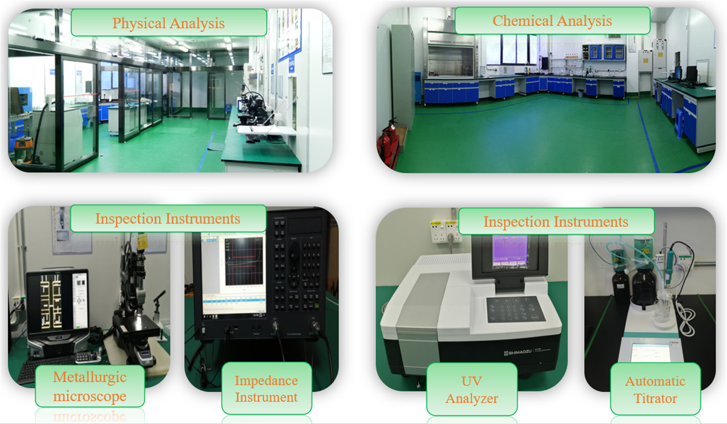
Of course, inspection and test are also highlight in quality management system of PCB ShinTech. We use these to make sure that our processes are running correctly. These steps give you the added re-assurance that the board you receive is correct to your design and will perform correctly over the lifetime of your product. We invested in equipment of X-ray fluorescent, AOI, fly probe testers, electrical tester and others for this purpose. Most customers do not have the resources to do things in-house. We take on the responsibility to ensure that every customer gets exactly what they need.
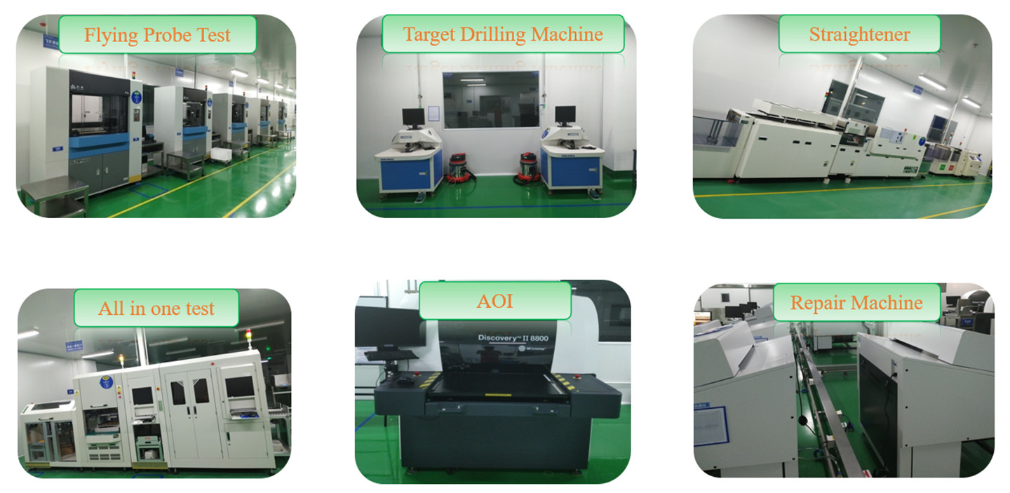
These steps are described as below.
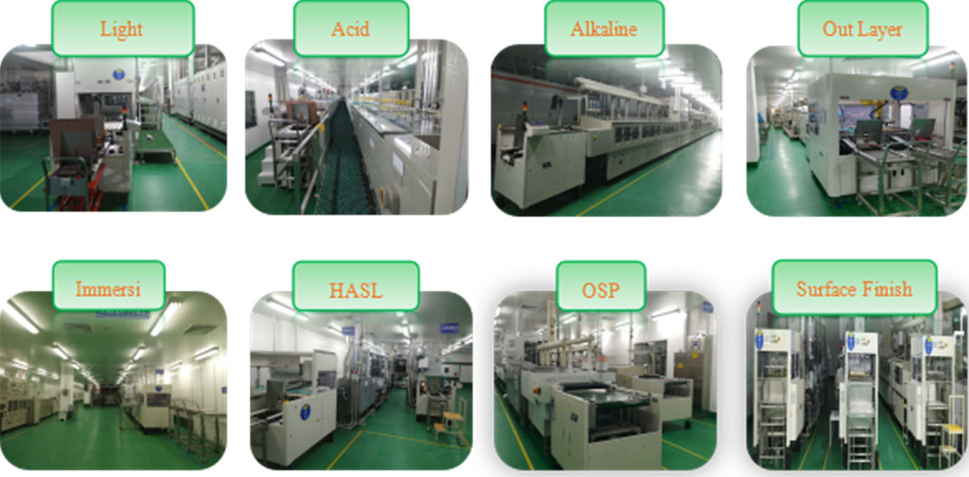
BARE PCB BOARD FABRICATION
● Automatic optical inspection (AOI) & visual inspection
● Digital microscopy
● Micro-sectioning
● Continuous chemical analysis of wet processes
● Constant analysis of defects and scrap with corrective actions
● Electrical test is included in all services
● Measurements for controlled impedance
● Polar Instruments software for design of controlled impedance structures and test coupons.
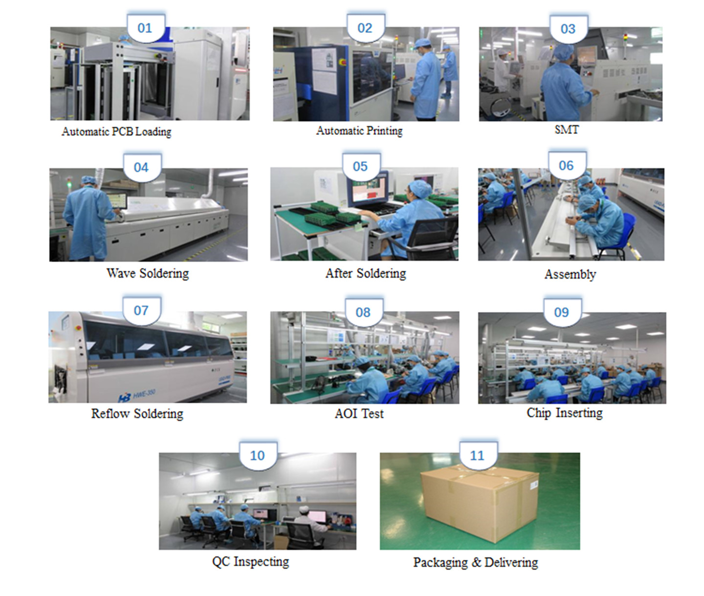
PCB ASSEMBLY
● Bare board and incoming component inspection
● First off checks
● Automatic optical inspection (AOI) & visual inspection
● X-ray inspection when required
● Functional testing when required
Facilities and Equipment
In-house facilities of PCB ShinTech are capable of 40,000 m2 per month of PCB fabrication. At the same time PCB ShinTech has 15 SMT lines and 3 through-hole lines in-house. Your PCBs are never produced by the lowest bidder out of a large pool of factories. To achieve exceptional quality performance from PCB assembly, we continuously invest in latest equipment that allows the exact precision necessary for the entire assembly process, including X Ray, solder paste, pick and place and more.
1. PCB
2. PCBA
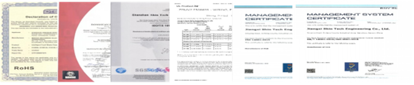
Certifications
Our facilities hold these certifications:
● ISO-9001: 2015
● ISO14001: 2015
● TS16949: 2016
● UL: 2019
● AS9100: 2012
● RoHS: 2015
Send your inquiry or quote request to us at sales@pcbshintech.com to get connected to one of our sales representatives who have the industry experience to help you get your idea to market.