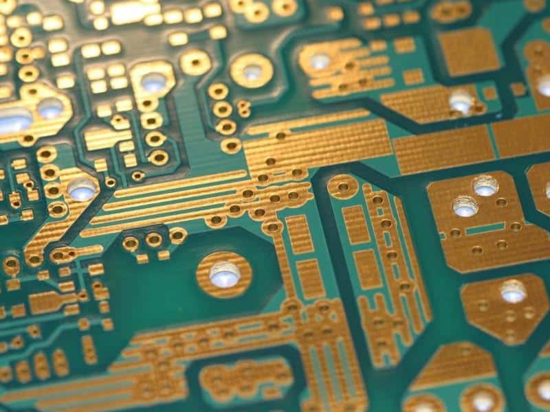
HDI PCB making in an automated PCB factory --- OSP surface finish
Posted: Feb 03, 2023
Categories: Blogs
Tags: pcb, pcba, pcb assembly, pcb manufacturing, pcb surface finish, HDI
OSP stands for Organic Solderability Preservative, also called circuit board organic coating by PCB manufacturers, is popular Printed Circuit Board surface finishing due to low costs and easy-to-use for PCB manufacturing.
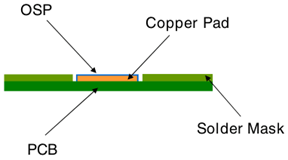
OSP is chemically applying an organic compound to exposed copper layer forming selectively bonds with copper before soldering, forming an organic metallic layer to protect exposed copper from rust. OSP Thickness, is thin, between 46µin (1.15µm)-52µin(1.3µm), measured in A° (angstrom).
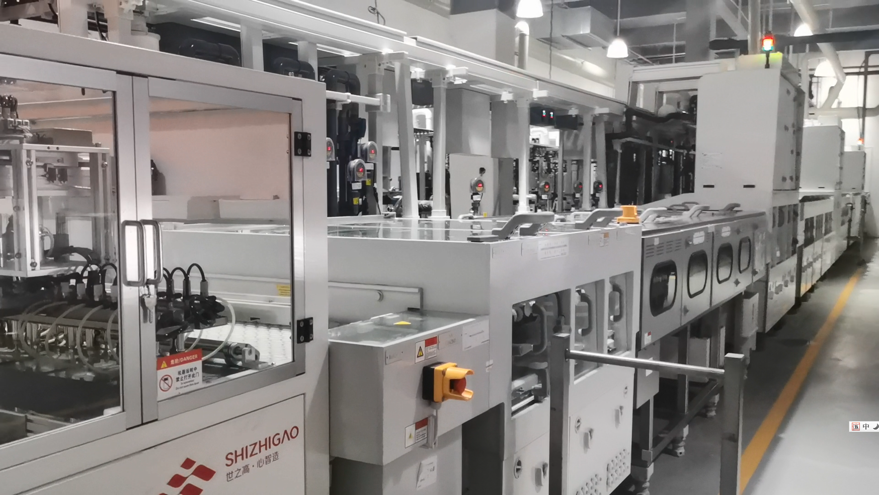
The Organic Surface Protectant is transparent, hardly for visually inspect. In the subsequent soldering, it will be quickly removed. The chemical immersion process can only be applied after all other processes have been done, including Electrical Test and Inspection. Applying an OSP surface finish to a PCB usually involves a conveyorized chemical method or a vertical dip tank.
The process generally looks like this, with rinses between each step:
1) Cleaning.
2) Topography enhancement: The exposed copper surface undergoes micro-etching to increase the bond between the board and the OSP.
3) Acid rinse in a sulfuric acid solution.
4) OSP application: At this point in the process, the OSP solution is applied to the PCB.
5) Deionization rinse: The OSP solution is infused with ions to allow for easy elimination during soldering.
6) Dry: After the OSP finish is applied, the PCB must be dried.
OSP surface finish is one of the most popular finishes. It is a very economical, environmentally friendly option for printed circuit boards manufacturing. It can provide co-planar pads surface for fine pitches/BGA/small components placement. OSP surface is highly repairable, and doesn’t demand high equipment maintenance.
However, OSP is not as robust as expected. It has its downsides. OSP is sensitive to handling and requires strictly handling to avoid scratches. Usually, multiple soldering is not suggested since Multiple soldering can damage the film. Its shelf life is the shortest among all surface finishes. The boards should be assembled soon after applying the coating. In fact, PCB providers can extend its shelf life by multiple redone the finish. OSP is very difficult to test or inspect due to its transparent nature.
Pros:
1) Lead-free
2) Flat surface, good for fine-pitch pads (BGA, QFP...)
3) Very thin coating
4) Can be applied together with other finishes (e.g. OSP+ENIG)
5) Low cost
6) Reworkability
7) Simple process
Cons:
1) Not good for PTH
2) Handling Sensitive
3) Short Shelf life (<6 months)
4) Not suitable for crimping technology
5) Not Good for multiple reflow
6) Copper will get exposed at assembly, requires relatively aggressive flux
7) Difficult to inspect, might cause issues in ICT testing
Typical use:
1) Fine pitch devices: This finish is best to apply to fine pitch devices because of the lack of co-planar pads or uneven surfaces.
2) Server boards: OSP’s uses range from low-end applications to high-frequency server boards. This wide variation in usability makes it suitable for numerous applications. It’s also often used for selective finishing.
3) Surface mount technology (SMT): OSP works well for SMT assembly, for when you need to attach a component directly to a PCB’s surface.
Back to Blogs
Post time: Feb-02-2023